💻💡 U.S. Pau Try Make Da ‘Chiplets’ Mo’ Power, Stay Top Notch In Tech 🇺🇸
No lie, da chiplets — how dem make da chips mo’ power — stay da main ting U.S. like do for industrial policy. But, brah, make more of dis kine stuff in da U.S. ain’t easy, yeah? 💪🏽🤔
For over 50 years, da guys who design da computer chips mostly went one way fo’ make ’em better: They made da electronic parts small kine so they could jam mo’ power into each piece of silicon. 🖥️🔬
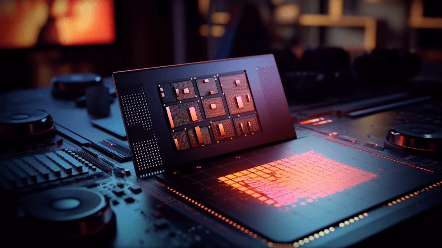
Den, like 10 years ago, da engineers at AMD, da chip maker, started fooling around with one new kine idea. Instead of making one big microprocessor with choke tiny transistors, they thought about making one from small kine chips, all packaged togedda tight tight, fo’ work like one electronic brain. 🧠💡
Dis idea, sometimes dey call ’em chiplets, it went big time. AMD, Apple, Amazon, Tesla, IBM, and Intel all went make dis kine stuff. Chiplets went popular fast kine, ’cause small chips cheaper for make, and bunches of ’em can beat da performance of any single piece of silicon. 📈🚀
Dis strategy, based on advanced packaging technology, now stay crucial fo’ da progress in semiconductors. And it stay one of da biggest changes in long time for da industry dat drives innovation in fields like artificial intelligence, self-driving cars, and military hardware. 🤖🚗💣
“Da packaging, das where da action stay going be,” said Subramanian Iyer, one professor of electrical and computer engineering at UCLA, who helped start da chiplet idea. “It’s happening ’cause no mo’ any other way.” 🎓🔌
But da trick part is dat dis kine packaging, like making chips, is mostly done by companies in Asia. Even though da U.S. make about 12% of da world’s semiconductors, American companies only make 3% of da chip packaging, according to IPC, one trade group. 🌏📊
Now, da issue wen put chiplets in da middle of U.S. industrial policy. Da CHIPS Act, one $52 billion package dat passed last summer, was seen as President Biden’s move fo’ make da domestic chip making more strong by providing money for build more hi-tech factories, or “fabs”. But part of it was also fo’ fire up advanced packaging factories in da U.S. to take more of dat crucial process. 🏭💰
“As chips get smaller, how you arrange da chips, which is packaging, become more and more important, and we need ’em done in America,” Commerce Secretary Gina Raimondo, wen say in one speech at Georgetown University in February. 🇺🇸🔬
Da Commerce Department now taking applications for manufacturing grants from da CHIPS Act, including for chip packaging factories. They also allocating money to one research program specifically on advanced packaging. 📚💵
Some chip packaging companies moving fast for da funding. One is Integra Technologies in Wichita, Kan., which announced plans for a $1.8 billion expansion there but said that was depending on getting federal subsidies. Amkor Technology, one Arizona packaging service that has most of its operations in Asia, also said it was talking to customers and government officials about a U.S. production presence. 🏢🏦
Da kine chip packaging ain’t new, and chiplets are just da latest version of dat idea, using new kine technology fo’ push da chips more close together — either side by side or stacked on top one another — plus get faster electrical connections between ’em. ⚡🔌
“What is unique about chiplets is da way dey are connected electrically,” said Richard Otte, da head honcho of Promex Industries, one chip packaging service in Santa Clara, Calif. 💼📍
Chips no can do nothing without one way fo’ connect ’em with other parts, which means dey need to be placed in some kind package dat can carry electrical signals. Dat process starts aftah da factories finish da first phase of manufacturing, which might create hundreds of chips on one silicon wafer. Aftah dat wafer is cut up, individual chips usually bonded to one key base layer called a substrate, which can carry electrical signals. 🔗📡
Den dey cover ’em in protective plastic, making one package dat can be plugged into a circuit board dat is crucial for connecting to other parts in a system. 🛡️🔋
Before, all dis kine processes needed plenty manual labor, so da Silicon Valley companies started moving packaging to countries in Asia where da wages stay lower, more than 50 years ago. Most chips are typically flown to packaging services in countries like Taiwan, Malaysia, South Korea, and China. 🛫🌍
Since den, packaging advances have become more important ’cause of da diminishing returns from Moore’s Law, da kine shorthand for chip miniaturization dat for decades drove progress in Silicon Valley. It is named after Gordon Moore, one co-founder of Intel, whose 1965 paper described how fast companies had doubled da number of transistors on a typical chip, which improved performance at a lower cost. 💸📈
But now days, smaller transistors not necessarily cheaper, partly ’cause building factories for top-notch chips can cost $10 billion to $20 billion. Big, complex chips also are costly to design and tend to get more defects, even as companies in fields like generative A.I. want more transistors than can currently be packed onto da biggest chips manufacturing machines allow. 🏭💔
“Da natural response to dat is putting more things in a package,” said Anirudh Devgan, big boss of Cadence Design Systems, whose software is used to design regular chips as well as chiplet-style products. 🎁📦
Synopsys, one rival, said it was tracking more than 140 customer projects based on packaging multiple chips together. As much as 80 percent of microprocessors will use chiplet-style designs by 2027, according to the market research firm Yole Group. 📊🚀
Now days, companies usually design all da chiplets in a package along with their own connection technology. But industry groups are working on technical standards so companies can more easily assemble products from chiplets that come from different makers. 🔄🔧
Da new technology mostly used now for extreme performance. Intel recently introduced a processor called Ponte Vecchio with 47 chiplets that will be used in one powerful supercomputer at Argonne National Laboratory, which is near Chicago. 🖥️💥🏙️
So, you see, bruddah, da U.S. stay focused on making ‘chiplets’ more power fo’ stay cutting-edge in tech. It’s all about working togedda, yeah? 🤝🌐🌈
NOW IN ENGLISH
💻💡 U.S. Aims to Supercharge ‘Chiplets’ to Maintain Dominance in Tech 🇺🇸
Chiplets, a method of designing high-performance chips, have become a pivotal part of U.S. industrial policy. However, promoting this activity domestically presents a significant challenge. 💪🔧
For over half a century, computer chip designers primarily relied on one strategy to boost performance: They miniaturized electronic components to pack more power onto each piece of silicon. 🖥️🔬
But more than a decade ago, engineers at the chip manufacturer Advanced Micro Devices (AMD) began to experiment with an innovative concept. Instead of designing a single large microprocessor filled with numerous tiny transistors, they proposed constructing one from smaller chips, tightly packaged together to function as a single electronic brain. 🧠💡
This idea, often referred to as chiplets, caught on rapidly. AMD, Apple, Amazon, Tesla, IBM, and Intel all introduced such products. Chiplets quickly gained popularity because smaller chips are less expensive to produce, and bundles of them can exceed the performance of any single slice of silicon. 📈🚀
This approach, rooted in advanced packaging technology, has become a vital tool for progress in the semiconductor industry. It signifies one of the most substantial shifts in years for a sector that fuels innovations in artificial intelligence, self-driving cars, and military hardware. 🤖🚗💣
“Packaging is where the action will be,” declared Subramanian Iyer, a professor of electrical and computer engineering at UCLA, who helped pioneer the chiplet concept. “It’s happening because there is no other way.” 🎓🔌
However, the problem is that such packaging, like the manufacturing of chips themselves, is mostly dominated by Asian companies. While the United States is responsible for approximately 12% of global semiconductor production, American companies account for just 3% of chip packaging, according to IPC, a trade association. 🌏📊
This issue has thrust chiplets into the heart of U.S. industrial policy. The CHIPS Act, a $52 billion subsidy package passed last summer, was perceived as President Biden’s effort to revitalize domestic chip production by funding the construction of more sophisticated factories, dubbed “fabs.” But it was also designed to stimulate advanced packaging factories in the United States to seize more of this essential process. 🏭💰
“As chips get smaller, the way you arrange the chips, which is packaging, becomes increasingly important, and we need it done in America,” Commerce Secretary Gina Raimondo, said in a speech at Georgetown University in February. 🇺🇸🔬
The Commerce Department is now accepting applications for manufacturing grants from the CHIPS Act, including those for chip packaging factories. It is also allocating funding for a research program focused on advanced packaging. 📚💵
Several chip packaging companies are moving swiftly to secure this funding. One such company is Integra Technologies in Wichita, Kan., which announced plans for a $1.8 billion expansion contingent on receiving federal subsidies. Amkor Technology, an Arizona-based packaging service with most of its operations in Asia, also mentioned it was discussing plans for a U.S. production presence with customers and government officials. 🏢🏦
Chip packaging is not a novel concept, and chiplets represent the latest iteration of this idea, using technological advances that allow the chips to be packed more densely — either side by side or stacked vertically — with quicker electrical connections between them. ⚡🔌
“What is unique about chiplets is the way they are connected electrically,” stated Richard Otte, the CEO of Promex Industries, a chip packaging service based in Santa Clara, California. 🏢⚙️
Without a means to connect with other components, chips are rendered useless, necessitating their placement in a package capable of transmitting electrical signals. This process commences once the initial phase of manufacturing is completed, which could generate hundreds of chips on a single silicon wafer. After this wafer is divided, individual chips are typically attached to a base layer known as a substrate, which can conduct electrical signals. 💡🔌
This combination is then encased in protective plastic, forming a package that can be integrated into a circuit board, a crucial step for connecting to other system components. 📦🔒
Originally, these processes required a significant amount of manual labor, leading Silicon Valley companies to outsource packaging to lower-wage countries in Asia over 50 years ago. Most chips are typically sent to packaging services in countries such as Taiwan, Malaysia, South Korea, and China. 🗺️🛫
Since then, packaging advancements have grown in importance due to the diminishing returns from Moore’s Law, the term for chip miniaturization that drove progress in Silicon Valley for decades. Named after Gordon Moore, a co-founder of Intel, Moore’s Law refers to his 1965 paper that described the rapid rate at which companies were doubling the number of transistors on a typical chip, improving performance at a reduced cost. 📉📚
However, smaller transistors aren’t necessarily cheaper these days, partly because building factories for cutting-edge chips can cost between $10 billion and $20 billion. Large, complex chips are also expensive to design and tend to have more manufacturing defects, even as companies in fields like generative A.I. desire more transistors than can currently be packed onto the largest chips that manufacturing machines permit. 🏭💰
“The natural response to that is putting more things in a package,” explained Anirudh Devgan, CEO of Cadence Design Systems, whose software is used to design conventional chips as well as chiplet-style products. 📦🖥️
Synopsys, a competitor, reported that it was tracking over 140 customer projects based on packaging multiple chips together. As much as 80% of microprocessors will use chiplet-style designs by 2027, according to the market research firm Yole Group. 📈🔮
Today, companies typically design all the chiplets in a package along with their own connection technology. But industry groups are working on technical standards to allow companies to more easily assemble products from chiplets that originate from different manufacturers. 🔄⚙️
The new technology is primarily used now for extreme performance. Intel recently introduced a processor called Ponte Vecchio with 47 chiplets that will be used in a powerful supercomputer at Argonne National Laboratory, located near Chicago. 🖥️💥
In summary, the U.S. is concentrating on enhancing the performance of ‘chiplets’ to maintain its leading edge in the tech industry. The focus is on unity and collaboration. 🤝🌐